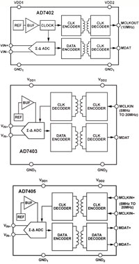
 The AD7402, AD7403, and AD7405 are high performance, second-order, Σ-Δ modulators that convert an analog input signal into a high speed, single-bit data stream with on-chip digital isolation based on ADI's iCoupler® technology. The modulators operate from a 4.5 to 5.5 V (VDD1) (AD7402) power supply or from a 5 V (VDD1) (AD7403/AD7405) power supply. The modulators accept a differential input signal of ±250 mV (±320 mV full scale). The differential input is ideally suited to shunt voltage monitoring in high voltage applications where galvanic isolation is required.
The analog input is continuously sampled by a high performance analog modulator and converted to a ones-density digital output stream with a data rate of 10 MHz (AD7402) or 20 MHz (AD7403/AD7405). The original information can be reconstructed with an appropriate digital filter to achieve 87 dB signal to noise ratio (SNR) at 39 kSPS (AD7402) or 88 dB signal-to-noise ratio (SNR) at 78.1 kSPS (AD7403/AD7405). The serial input/output can use a 3 V to 5.5 V or a 3.3 V supply (VDD2) (AD7402) or 5 V or a 3 V supply (VDD2) (AD7403). The LVDS input/output can use a 5 V or a 3.3 V supply (VDD2) (AD7405).
The serial and LVDS interfaces are digitally isolated. This combined with monolithic transformer technology, means the on-chip isolation provides outstanding performance characteristics; superior to alternatives such as optocoupler devices. The AD7402 and AD7403-8 devices are offered in an 8-lead wide body SOIC package and have an operating temperature range of -40°C to 105°C. The AD7403 and AD7405 devices are offered in a 16-lead, wide-body SOIC package and have an operating temperature range of -40°C to 125°C.
| Features and Benefits |
|
|
- 10 MHz internal clock rate (AD7402)
and 5 MHz to 20 MHz external clock input rate (AD7403/AD7405)
- 16-bits; no missing codes
- Signal-to-noise ratio (SNR): 87 dB typical (AD7402) and 88 dB typical (AD7403/AD7405)
- Effective number of bits (ENOB): 13.5 bits typical (AD7402) and 14.2 bits typical (AD7403/AD7405)
- Typical offset drift vs. temperature: 1.7 µV/°C (AD7402), 1.6 μV/°C (AD7403/AD7405), 2 μV/°C typical (AD7403-8)
|
|
- Serial (AD7402/AD7403) and LVDS (AD7405) interfaces
- On-board digital isolator
- On-board reference
- Full-scale analog input range: ±320 mV
- -40°C to 105°C (AD7402/AD7403-8) and -40°C to 125°C (AD7403/AD7405) operating ranges
- High common-mode transient immunity: >25 kV/μs
- 8-lead (AD7402/AD7403-8) and 16-lead (AD7403/AD7405), wide-body SOIC, with increased creepage package
|
| Applications |
|
|
- Shunt current monitoring
- AC motor controls
- Power and solar inverters
|
|
- Wind turbine inverters
- Data acquisition systems
- Analog-to-digital and opto-isolator replacements
|
 The AD7402, AD7403, and AD7405 are high performance, second-order, Σ-Δ modulators that convert an analog input signal into a high speed, single-bit data stream with on-chip digital isolation based on ADI's iCoupler® technology. The modulators operate from a 4.5 to 5.5 V (VDD1) (AD7402) power supply or from a 5 V (VDD1) (AD7403/AD7405) power supply. The modulators accept a differential input signal of ±250 mV (±320 mV full scale). The differential input is ideally suited to shunt voltage monitoring in high voltage applications where galvanic isolation is required.


