מק"ט יצרן # ICE40LP384-SG32
IC FPGA 21 I/O 32QFN
Lattice Semiconductor Corporation
Microcontrollers have tons of useful peripherals; GPIO, timers, UART, SPI, and I2C are such useful peripherals that they come on nearly every microcontroller these days. Niche peripherals like LCD drivers, internal op-amps, or CAN transceivers can, on the right project, reduce cost, complexity, and component count. But none, IMHO, are quite as versatile as the configurable logic block (CLB) from Microchip.
The CLB from Microchip (found on PIC16F131xx devices) is an example of an MCU peripheral that gives the designer a small piece of configurable digital logic inside their microcontroller.
 From Microchip, Custom Logic Peripherals
The CLB contains a handful of logic elements (not unlike the dozens or thousands of logic elements that make up the internal fabric of an FPGA) that each implement a specific logic device: an AND gate, a multiplexer, a D flip-flop, a JK flip-flop, etc. The inputs to these blocks can come from a number of different signal sources inside the microcontroller (e.g., from a GPIO pin, from an internal timer, etc.), and the outputs can also go to many different signal sinks (e.g., to a GPIO pin, to an interrupt signal, to another CLB logic element, etc.).
Microchip also offers a peripheral called the configurable logic cell (CLC) on most (all?) of their PIC16F and PIC18F devices (along with two PIC10s and one PIC12) and another called the configurable custom logic (CCL) on most (all?) of their AVR devices.


These peripherals act exceedingly similarly to the CLB, with slight differences in which logic devices are supported (notice that the CLC and CCL can each implement an SR latch, which the CLB cannot) and also where the inputs and outputs can be routed from/to.
Although simple in their design, these peripherals can punch way above their weight class, helping to create highly complex systems that shift some of the software load or component count of a project onto small digital logic circuits.
We're about to see the power of digital logic, so let's dust off those digital logic design skills!
Can you create digital designs that implement the following functionalities?
1. 4-input priority encoder (solutions can be found at the end of the post)

2. Toaster FSM (solutions can be found at the end of the post)

A handful of gates and flip-flops might not seem like much, but there is lots that they can do to help offload computation load or decrease component count in a final design. Here are some simple applications.
(From Microchip document DS41631B, "Configurable Logic Cell Tips ’n Tricks")
A "normal" bitstream will represent 1s and 0s as static signal levels. Consider a TTL-UART signal: 1s are 3.3/5V and 0s are 0V. The value 1010011 (MSB-first) would look like this (where each column represents half of the clock period):

A Manchester-encoded signal, however, represents 0s as low-to-high transitions and 1s as high-to-low transitions (using traditional encoding; IEEE 802.3 associates 1s and 0s in the opposite manner, which makes a little more sense to me). The same value as before, when Manchester-encoded, would look like this:

Manchester-encoded signals have the benefit of being self-clocking and also have no DC signal bias, allowing the signal to be AC-coupled. These features are preferred for communications requiring only a single transmission channel (such as wireless communications) or that operate in noisy environments.
We can use a CLB to convert a clock and bitstream into a Manchester-encoded signal using just an XOR gate.

(From Microchip appnote AN2133, "Extending PIC MCU Capabilities Using CLC")
An emergency shut-off is a necessary precaution for systems that are controlling heavy machinery (or, really, anything that could cause human or collateral damage if misused).

For example, by feeding the outputs of two analog comparators into the CLC above, we can detect when temperature or pressure exceeds or falls below a safe threshold and generate a shutdown command accordingly. Using the CLC, we can combine these signals in a number of ways. The shutdown command generated by the CLC could be set by ANDing the comparators, by ORing them, or it could even be configured as the output of an SR latch, which is set by an ORing of the two comparators, which would result in the shutdown command being held high even if the temperature and pressure returned to normal levels. This could ensure that the system remains off until a human operator determines that it can be restarted safely by resetting the SR latch. For more complex behaviors, you could even construct an FSM inside the CLC (see here for an example FSM design using the CLC).
Because this is done completely in hardware, it stands a much better chance of passing a safety-critical verification than if the emergency shut-off were detected via software.
But the fun doesn't stop there! Here are a few more complex applications for the CLB.
This one comes from a contest that Microchip held earlier this year to find the most creative use of the CLB. Using all 32 elements in the CLB on a PIC16F13145, Mark Omo built a DAC that had an amazing 480 Hz BW, surpassing both PWM and R2R DACs in their performance! It was even capable enough to stream audio from his PC.
Another finalist in that Microchip CLB contest built a SIRC (Sony Infrared Remote Control) encoder/decoder for playing laser tag.

Although generating and detecting SIRC signals could have been very software-intensive, the CLB was used to completely offload those operations to hardware. The best part is that the CLB implementation includes a UART API, allowing shots to be triggered by a UART command byte and for shot detection to be sent back over that same UART port!
Such as:
If you like the idea of configurable logic alongside your microcontroller but don't see yourself using a PIC16 or AVR device in the near future, there are still plenty of ways you can incorporate capabilities like this in your next project.
Many (but not all) of the Cypress PSoC family of microcontrollers have configurable logic blocks called universal digital blocks (UDB).
 From the "PSoC 4 Architecture Technical Reference Manual"
The UDBs each contain two PLDs that are noticeably more capable than Microchip's CLB. The PLDs inside each UDB are formed from a 12-term AND-matrix followed by an 8-term OR-matrix (similar to the old PLAs), which is then routed to a macrocell. The macrocell can keep the output un-registered (i.e. combinational) or it can store the output of the OR gate in either a D or T flip-flop. The macrocell also implements carry logic between the macrocells as well as various reset functions.
The "Datapath" element is an interesting addition, as it contains an ALU to more efficiently implement arithmetic functions.

The TI C2000 family of microcontrollers contain their own configurable logic blocks, that are also quite a bit more capable than the CLBs from Microchip.
 From TI Resource Explorer: Configurable Logic Block (CLB)
The CLB on a C2000 microcontroller contains up to 8 tiles, with each tile containing the following submodules:
The inputs to each submodule can come from any of the other LUTs, FSMs, or counter submodules within that tile or from up to 8 other signals in the system, allowing for an enormous degree of configurability.
Of course, the ubiquitous piece of configurable digital logic is the FPGA, which we could always add to our microcontroller externally.

Everything that FPGAs are famous for (soft-core CPUs; fast, custom digital logic; etc.) would be available to your embedded system, in that case! And it wouldn't necessarily need to be pricey, either: ice40 FPGAs with 48 logic elements can be had on DigiKey for a low cost, even in single quantities.
The main advantage of this approach is that we can now add configurable digital logic to any MCU. The main disadvantages are
Another option for external programmable logic is a CPLD. CPLDs are more complex than a PLA (which are built using AND-OR matrices, like what we saw above inside the PLDs in the Cypress UDBs) and less complex than an FPGA. The main difference between CPLDs and FPGAs seems to be the ways in which
For FPGAs, the individual logic elements are loaded at start-up from non-volatile memory with the LUT pattern that defines each block. Blocks are connected locally to each other, so signals that travel from one side of the FPGA to the other generally have to pass through other logic blocks along the way.

This makes FPGAs ideal for designs that need LOTS of logic elements and the higher capability that comes with that.
For CPLDs, on the other hand, individual logic elements (called "macrocells") use internal Flash memory or fuse bits to set the pattern of AND and OR terms that define the custom logic (though some do use LUTs, like FPGAs). The input pins on a CPLD and the outputs of all of the macrocells are connected to an enormous matrix which allows any of them to be used as inputs to each AND matrix (or LUT).

This makes CPLDs lower power and faster to start-up than FPGAs, with more predictable timing, also. CPLDs also do not require any external non-volatile memory, like FPGAs do, and typically require only a single voltage level to power them (FPGAs often require several). However, it also limits how many macrocells a CPLD could feasibly contain (the interconnect matrix would be infeasibly huge for CPLDs with several thousand macrocells). CPLDs are priced similarly to FPGAs; CPLDs containing 64 macrocells can be had on DigiKey for $2.40 in single quantities.
Interestingly, all of the options above are quite a bit more powerful than the Microchip CLBs.
"Wait, I could build a laser tag system with the CLBs; what could I do with 32 macrocells/logic elements?!"
LOTS. For example, a minimal 8-bit CPU. Imagine that: for just a few dollars, you could add a small co-processor to your embedded system. Not bad, eh?
And now, let's put some of this new knowledge into practice!
In what ways could the following systems benefit from a piece of configurable digital logic?
Adding a small piece of digital logic to your embedded system can be a very useful thing! Hardware implementations of functions like FSMs or Manchester encoding can operate much faster, be much more reliable, and operate at lower power than software implementations. My favorite way to do this is with the CLB/CLC/CCL peripherals from Microchip. Although they are less capable than other options, they are also simpler and still able to implement some very useful functions. Other ways to add configurable digital logic include using a Cypress PSoC microcontroller, a TI C2000 microcontroller, or using an external FPGA or CPLD. All four of those last options are quite a bit more complex (and also capable) than the Microchip CLB, though.
And I've one last challenge question for you!
List three or more things you've learned (or were reminded of) while reading this article.
If you've made it this far, thanks for reading and happy hacking!

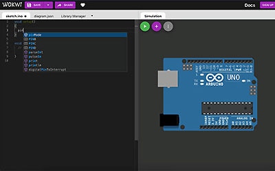
See it in simulation here.

Some things that a CLB/CPLD could do include:
Some things that a CLB/CPLD could do include: